Doodling Shake Bot DIY STEM Kit
$9.99$4.95
Posted on: May 8, 2006

For the first time, researchers have directly measured the electronic structure of individual carbon nanotubes whose physical properties had already been determined. This new study, pioneered by researchers at the U.S. Department of Energy’s Brookhaven National Laboratory working with their colleagues at Columbia University, may help scientists determine the usefulness of carbon nanotubes in various applications, from microelectronics to mechanical, thermal, and photovoltaic devices. The researchers report on their work in the April 28 issue of Science.
“This combined study technique allows us -- for the first time -- to test some fundamental predictions about nanotube behavior,” said Matt Sfeir, a physicist in Brookhaven’s Condensed Matter Physics and Materials Sciences Division and lead author of the study. “Understanding how these materials function on a basic level is key to controlling and manipulating them for future successful commercial applications.”
Carbon nanotubes are capsule-shaped molecules only a few billionths of a meter (nanometers) in width. In nanotube form, many materials take on useful, unique properties, such as physical strength and excellent conductivity. Single-walled carbon nanotubes are the most widely investigated variety, but what makes them so interesting also makes them very difficult to study -- several hundred distinct species exist, and each has dramatically different electronic properties thought to be linked to their unique individual structure.
Sfeir and his colleagues sought to look at both the structure of carbon nanotubes and their corresponding electronic properties using two existing techniques. The twist is that the two techniques would be used on each of the nanotubes studied, giving the researchers a complete picture of their unique structure and behavior as well as greater knowledge about how they “transition” from semi-conducting to metallic in terms of their electronic properties.
The work started at Columbia, where the single-walled carbon nanotubes were grown freely suspended over a slit etched into a silicon substrate. The researchers then identified usable individual nanotubes, labeled them, and studied them with a technique known as resonance Rayleigh scattering. This method allows researchers to detect the optical spectrum of light scattered from the nanotubes and use that scattered light to determine their electronic structure.
“The optical spectra alone, however, does not give us sufficient information to absolutely assign electronic transitions to the nanotubes’ physical structure,” said Sfeir. “We needed a technique that could provide independent structural verification. Fortunately, our colleagues in the electron microscopy group at Brookhaven were interested in this problem as well and were able to provide a solution - electron diffraction.”
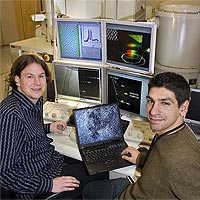
The labeled nanotubes were brought to Brookhaven, where physicist Tobias Beetz subjected them to electron diffraction studies using an electron microscope. This gave the researchers complementary data on the nanotubes’ physical structure.
“Electron diffraction is an ideal tool for determining the exact structure of metallic and semiconducting nanotubes,” said Beetz. “We can use this tool to easily see if we are dealing with single-walled or double-walled nanotubes, and we are not limited to studying a certain nanotube diameter range as we would be using other methods.”
After collecting these two sets of information from many different nanotube structures, researchers were then able, for the first time, to test theories of nanotube electronic transitions and confirm several assumptions made in previous models.
“One aspect we have verified is how small changes in the pitch of the hexagons on the nanotube sidewall, determined by how the nanotube grows, lead to systematic deviations in the electronic behavior in both semi-conducting and metallic structures,” said Sfeir. “This predicted behavior, known as the “family pattern,” had never before been directly tested, and our experimental results place it on a solid foundation that was previously lacking.”
This research was funded by the Office of Basic Energy Sciences within the Department of Energy’s Office of Science, the National Science Foundation, and the New York State Office of Science, Technology, and Academic Research (NYSTAR).